August 28, 2026
DIC EXPO 2026 | Jingce Unveils "AI+Metrology & Inspection" Products, Ushering in a New Era of Yield Management for the Full Display Industry



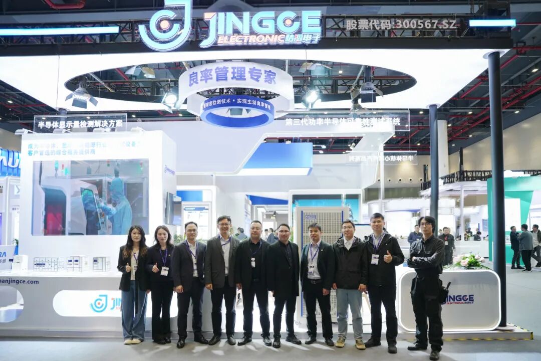
The 2026 Jiufeng Mountain Forum grandly kicked off at Wuhan Optics Valley Science and Technology Exhibition Center from April 23 to 25. Focusing on cutting-edge fields including SiC/GaN, optoelectronics, AI computing power and new energy, the forum opened a new chapter for the development of compound semiconductors.

As a leading domestic enterprise in semiconductor metrology and inspection technologies, Jingce made a stunning debut with power semiconductor test solutions, a full range of core semiconductor devices, as well as semiconductor display metrology and inspection solutions, demonstrating its industrial upgrading path from "Precise Metrology & Inspection" to "Proactive Yield Management".
Currently, the global semiconductor industry is embracing a new round of technological revolution and industrial restructuring led by compound semiconductors. Represented by SiC and GaN, third-generation semiconductors break through the performance limits of traditional silicon-based semiconductors with superior characteristics such as high frequency, high power, high voltage resistance, high temperature resistance and excellent optoelectronic performance. They have become the core support for strategic industries including 5G/6G communications, new energy vehicles, AI data centers and next-generation displays. However, higher standards are set for their reliability verification. Particularly in automotive-grade applications, reliability serves as a pivotal factor in the R&D and industrialization of third-generation semiconductors.
To cater to the rigorous testing requirements of third-generation semiconductors, Jingc provides multi-scenario test solutions integrating dynamic burn-in test, static burn-in test and bipolar degradation test for third-generation power semiconductors. The solutions deliver outstanding performance in core indicators such as test accuracy, reliability, compatibility and intelligence. Drawing on mature engineering experience, serialized product matrix and customized solutions, the company satisfies customers’ demands for complete and reliable mass production testing.
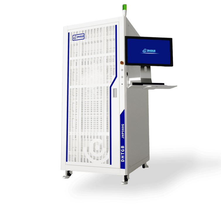
JHP560SeriesDynamic Reliability Test System for Third-Generation Power Semiconductors
Jingce’s JHP560 series dynamic reliability test system for third-generation power semiconductors simulates high-temperature, dynamic and high-frequency AC switching environments consistent with actual working conditions. Featuring large-capacity and high-performance testing capacity, it accurately captures early failure risks caused by gate oxide defects, interface state degradation, intrinsic material defects and other issues, enabling efficient evaluation and screening of device reliability, and effectively improving device yield and long-term stability.
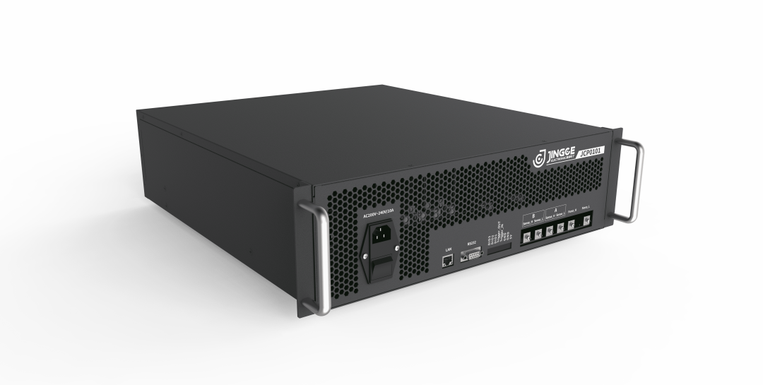
In addition, the JHP560 series is equipped with an in-house developed 8-channel high-current narrow pulse source, which perfectly matches the high-speed, high-voltage and high-current characteristics of third-generation power semiconductors. Centered on ultra-fast response, ultra-high precision and multi-channel coordinated testing, it delivers efficient and reliable one-stop testing services for customers’ device R&D and mass production inspection.
Taking independent innovation as the core and industry-university-research cooperation as dual driving forces, Jingce relies on its full-stack self-developed "Optical - Mechanical - Electrical - Algorithm - Softare" integrated technology platform. The company has built a full-process metrology and inspection product system covering front-end semiconductor manufacturing, advanced packaging and post-process inspection. It has also made strategic layout of core devices including film thickness gauges, ellipsometers and source meters, providing comprehensive metrology and inspection technical services for the entire semiconductor industrial chain from silicon wafers, wafers to chips.
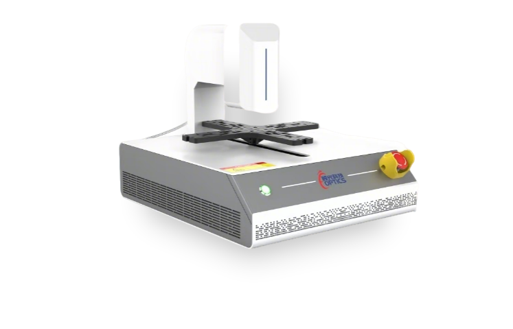
As universally recognized core next-generation optoelectronic technologies, Micro-LED and OLED semiconductor displays feature disruptive strengths including ultra-high brightness, extreme energy efficiency and ultra-long service life, making them ideal solutions to address future scenarios such as automotive intelligent light effects and high-end displays. With in-depth layout across the full AR/VR/MR industrial chain, Jingce has developed full-process semiconductor display metrology and inspection solutions to efficiently advance the industrialization of cutting-edge next-generation display technologies.
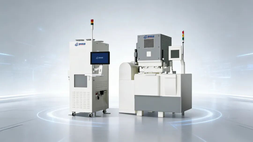
Prober ATE Inspection Equipent
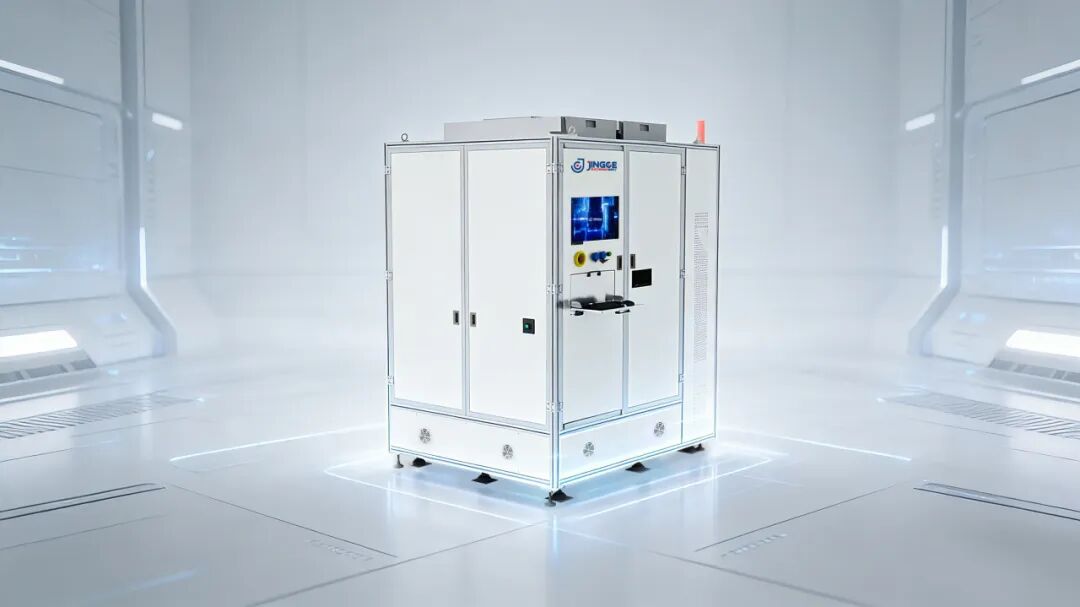
Prober AOI Inspection Equipment
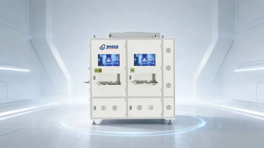
Gamma Carlibration Equipment
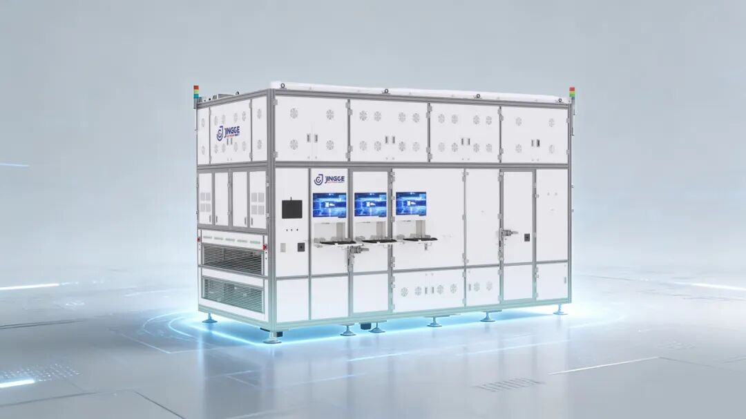
SLT AOI Inspection Equpment
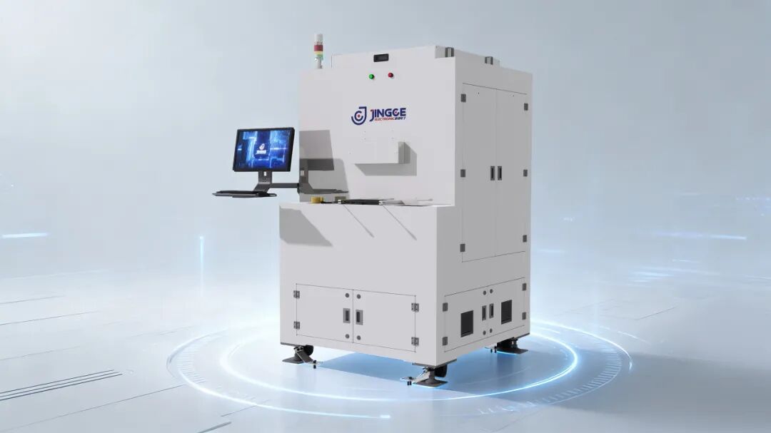
NED AOI Inspection Equipment
Jingce ’s semiconductor display metrology and inspection solutions innovatively integrate probe station ATE test equipment, probe station AOI inspection equipment, Gamma calibration equipment, SLT AOI inspection equipment and NED AOI inspection equipment, forming full-process metrology and inspection capabilities covering wafer electrical sorting, optoelectronic testing with precision instruments, near-eye displays and finished product performance verification.
Deep integration of AI and metrology & inspection realizes pixel-level color management, high-precision spectral analysis and intelligent judgment of appearance defects, forming a closed-loop of full-link data. It delivers a highly scalable technical platform to meet metrology and inspection demands of semiconductor displays and flexible display devices, and provides robust support for customers covering the whole process from chips to modules.
Its participation in the 2026 Jiufeng Mountain Forum serves as a vital platform for Jingce to deepen industrial collaboration and showcase technological prowess. Supported by solid technological accumulation and industrial experience, the company takes an active part in frontier industrial exchanges, comprehensively demonstrating innovative breakthroughs and core industrial value of semiconductor metrology and inspection. With leading process inspection and yield management capabilities, it continues to fuel the development of the semiconductor industry, standing out as a highly sought-after semiconductor metrology and inspection technology service provider at the exhibition.