June 26, 2026
2026 Automotive Testing Expo | Jingce Electronics Presents Innovative Automotive Electronic Testing Achievements to Continuously Drive High-Quality Industrial Development




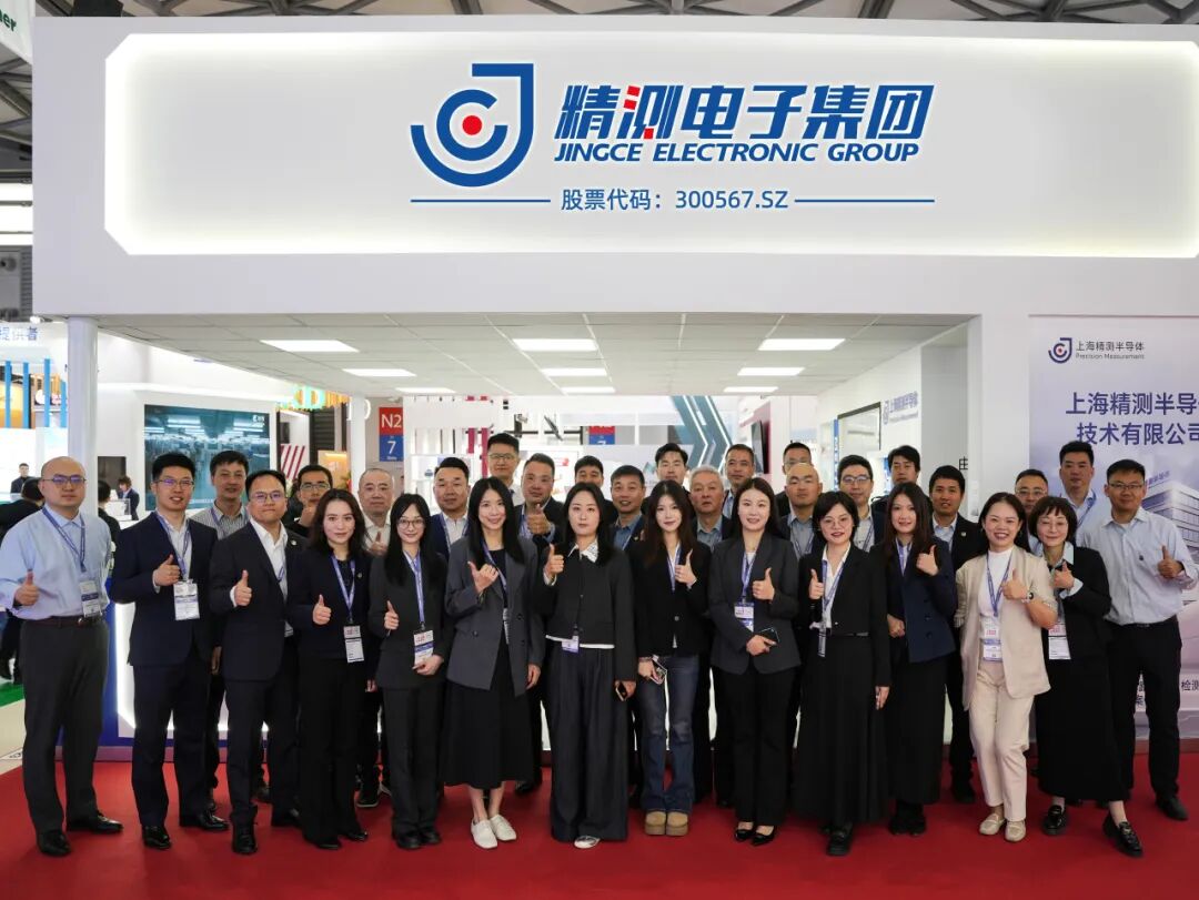
From March 25 to 27, SEMICON CHINA 2026, the world’s largest, highest-profile and most influential semiconductor industry exhibition, grandly opened at Shanghai New International Expo Centre.
Currently, the technology revolution represented by AI is profoundly reshaping the landscape of the global semiconductor industry. The race for AI computing power has not only driven chips toward more advanced process nodes, but also spurred rapid iterations of core technologies such as High Bandwidth Memory (HBM) and advanced packaging. Caught between explosive technological advancement and mounting cost pressures, the industry’s core priority for breakthrough has become "boosting performance, raising yield and cutting costs". Stricter standards are being imposed on chip testing precision, process control and yield management, bringing unprecedented development opportunities as well as challenges to manufacturers of semiconductor metrology and inspection equipment.
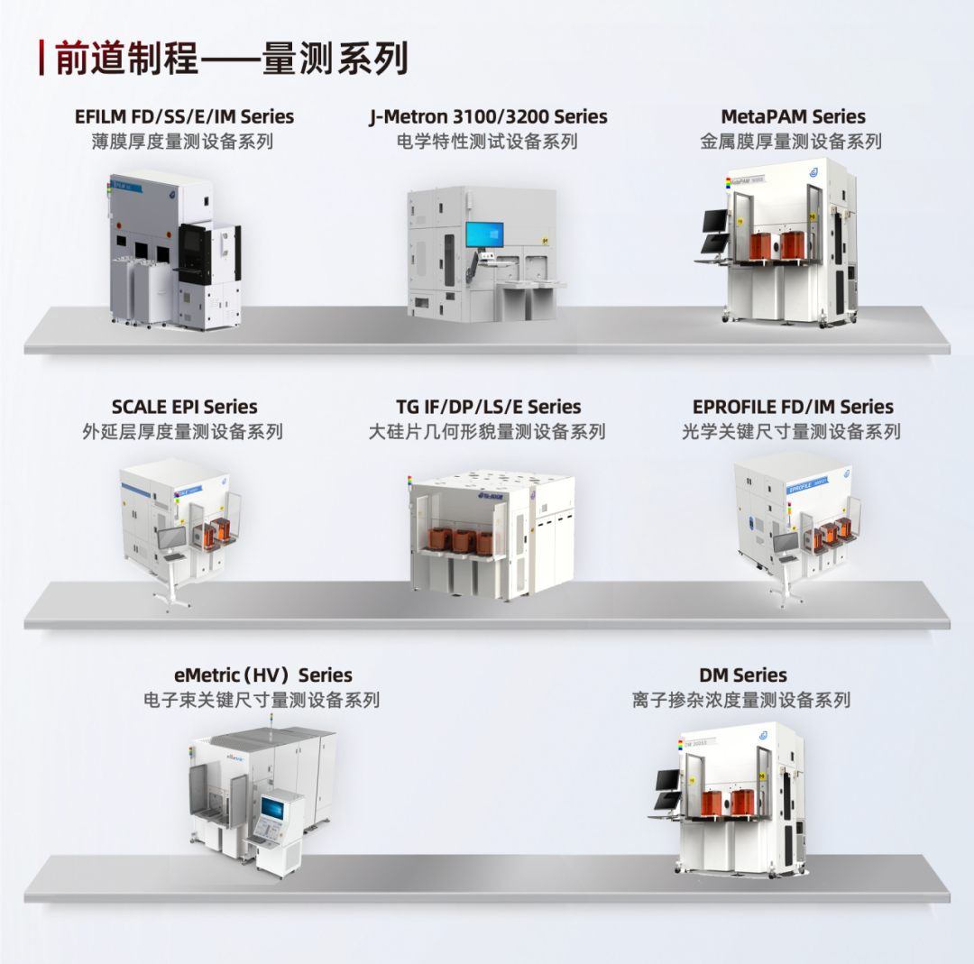
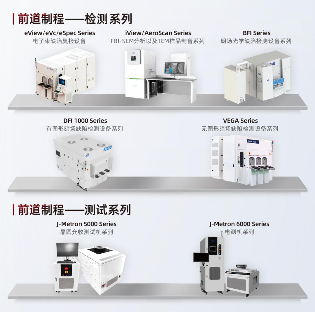
Jingce has long focused on metrology and inspection for integrated circuit manufacturing, mastering pivotal core technologies including spectral scatterometry, optical interferometry, optical microscopic imaging, electron/ion beam imaging and electrical testing. It has built 18 product clusters and over 40 product lines covering metrology, inspection and testing for semiconductor front-end processes, with its relevant products and technologies ranking among the domestic industry’s leaders and delivering distinct competitive advantages.
At this exhibition, aligned with critical front-end process nodes, the company showcased a lineup of domestically produced metrology and inspection equipment featuring high precision, exceptional stability and broad compatibility. Multiple new products made their debut, including the eMetric 2000 Series electron beam linewidth metrology system, J-Metron 5400 Series 100-pin WAT electrical signal tester, BFI 200 Series patterned wafer defect inspection system and Vega 500 Series bare wafer defect inspection system.
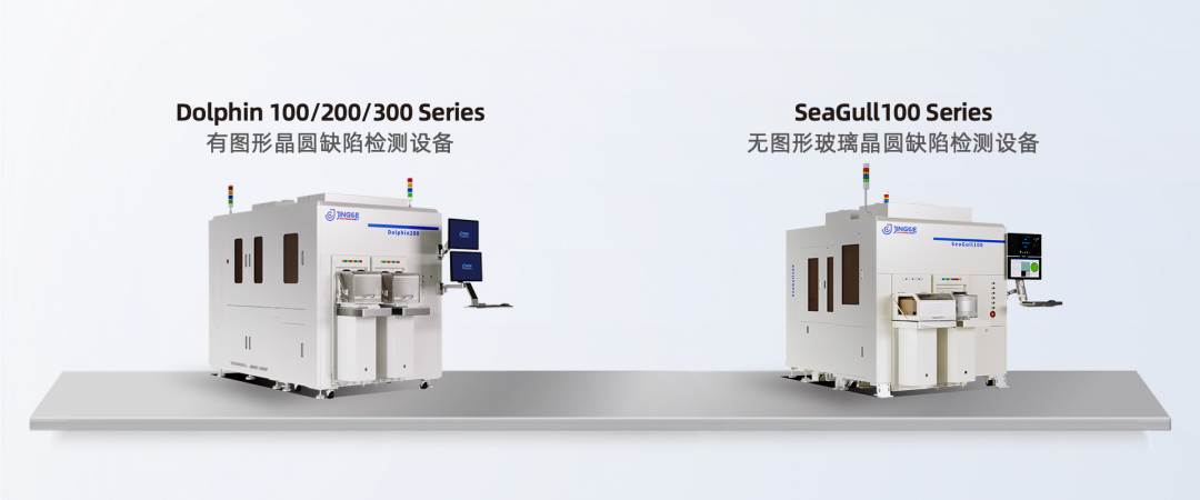
To address challenges posed by 2.5D/3D advanced packaging, Jingce has rolled out product lines for patterned wafer defect inspection and bare glass wafer defect inspection.These systems detect and measure submicron-level wafer defects by integrating high-precision bright/dark field imaging and professional defect inspection algorithms. They can also be upgraded to support wafer bumping and Micro-LED 3D metrology, effectively boosting clients’ manufacturing capacity and production efficiency while precisely accommodating complex defect inspection demands arising from the rapid evolution of advanced packaging.
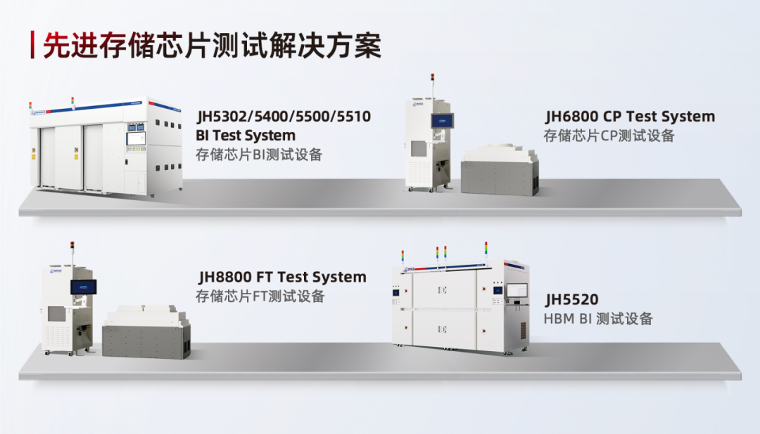
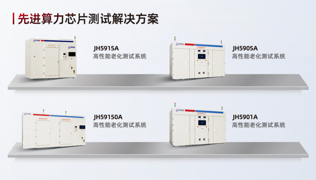
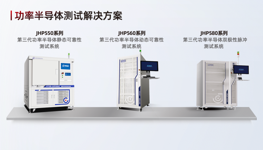
Continuously investing in Automatic Test Equipment (ATE), Jingce Electronic has established a full-scenario testing ecosystem covering advanced memory, high-performance computing and third-generation power semiconductors, delivering customized, efficient and reliable testing solutions for clients across diverse sectors. For advanced memory chips, the company provides integrated multi-scenario testing solutions combining Burn-In (BI), Chip Probing (CP) and Final Test (FT). These solutions have been upgraded to support FT for UFS 4.1, with adaptation for UFS 5.0 currently underway. In addition, the brand-new JH5520 HBM BI test system has been launched to precisely meet testing requirements for high-end HBM memory.
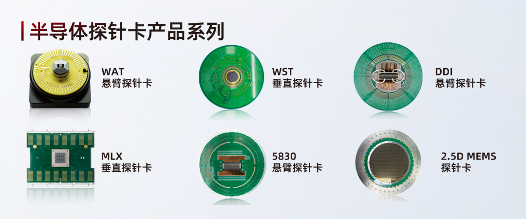
In the semiconductor probe card segment, Jingce Electronic has achieved core breakthroughs spanning basic probes to complete probe card assemblies. Its product portfolio includes cantilever probe cards, 2D MEMS probe cards, 2.5D MEMS probe cards and WAT probe cards, fully covering test applications for display driver ICs, memory chips, domestic GPUs and AI chips. All products are independently developed in-house to ensure supply security and controllability.
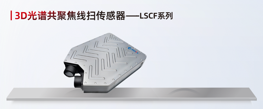
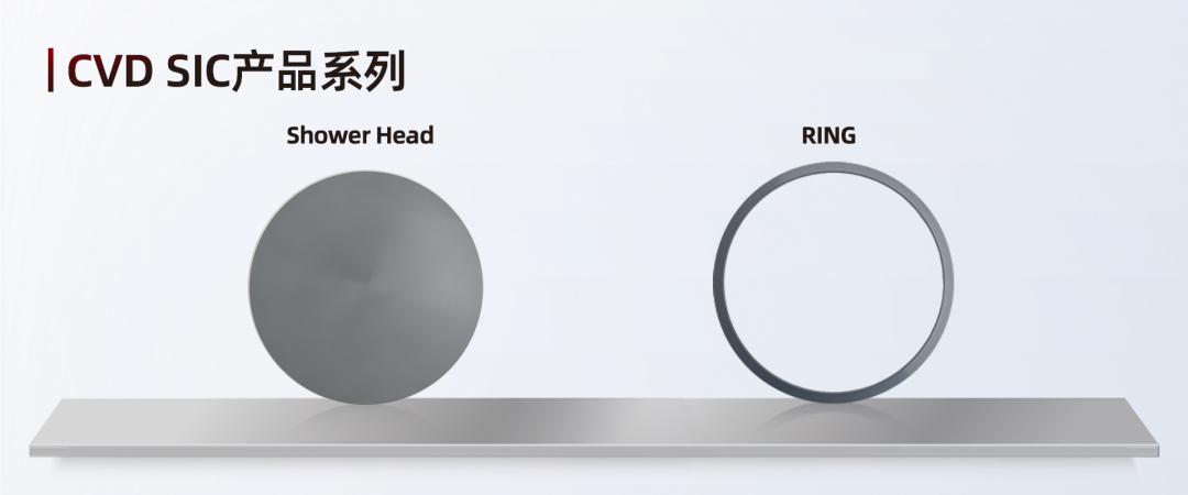
Meanwhile, Jingce Electronic has expanded its layout into silicon carbide (SiC) material spare parts for semiconductors and precision optical instruments — namely 3D line-scan spectral confocal sensors. Its CVD SiC product series covers core components such as rings and shower heads, widely adopted in semiconductor packaging and power device substrates. The 3D line-scan spectral confocal sensor delivers submicron-level high precision, enabling rapid measurement of 3D topography, dimensional tolerances, surface defects and layered material tomography for chip electrodes, pins, packaging units and wafer defect inspection.
Jingce Electronic’s participation in SEMICON CHINA 2026 serves not only as a vital platform to showcase its technological prowess in semiconductor metrology & inspection as well as its full-spectrum product portfolio, but also as a critical opportunity to extensively connect with the global semiconductor industrial chain, gain insights into cutting-edge industry trends, and deepen collaboration with upstream and downstream partners.
Leveraging its full-stack self-developed integrated technology platform that integrates optics, mechanics, electronics, computing and software, Jingce Electronic has built an intelligent inspection ecosystem covering precision metrology instruments, smart inspection equipment and industry-specific solutions. It delivers comprehensive metrology and inspection technical services throughout the entire semiconductor chain, ranging from silicon wafers and patterned wafers to finished chips. Backed by leading process inspection and yield management capabilities, the company continuously empowers the advancement of the semiconductor industry.
Beyond mere inspection, we deliver proactive yield management. Moving forward, Jingce Electronic will remain focused on independent innovation as its core driver and keep deepening its presence in the semiconductor sector. Riding the technological waves of AI, high-performance computing and advanced memory, the company will continuously push the boundaries of metrology and inspection technologies, further perfect its full-range metrology & inspection solutions, and strengthen synergetic cooperation with upstream and downstream partners across the industrial chain. It will provide customers with more precise, efficient and value-adding yield management solutions, helping the global semiconductor industry embrace a higher-quality future.
Jingce’s participation in SEMICON CHINA 2026 serves not only as a vital platform to showcase its technological prowess in semiconductor metrology & inspection as well as its full-spectrum product portfolio, but also as a critical opportunity to extensively connect with the global semiconductor industrial chain, gain insights into cutting-edge industry trends, and deepen collaboration with upstream and downstream partners.
Leveraging its full-stack self-developed integrated technology platform that integrates optics, mechanics, electronics, computing and software, Jingce Electronic has built an intelligent inspection ecosystem covering precision metrology instruments, smart inspection equipment and industry-specific solutions. It delivers comprehensive metrology and inspection technical services throughout the entire semiconductor chain, ranging from silicon wafers and patterned wafers to finished chips. Backed by leading process inspection and yield management capabilities, the company continuously empowers the advancement of the semiconductor industry.